
Google's headline says "new TPUs," but the two products are different kinds of things. TPU 8tx uses the same silicon as TPU 8t. TPU 8i Max puts two TPU 8i chips in one package. Google did not build another chip. It rearranged the packaging, host CPU, network, security and software around existing chips to make a new system.
The 9 November 2026 announcement says this directly. Chip design takes years, but a system is a question of how compute, networking and storage are bound together, so a new configuration can arrive in months. The signal is that infrastructure competition in the agent era is moving from the chip to the system envelope.
Four systems, one portfolio
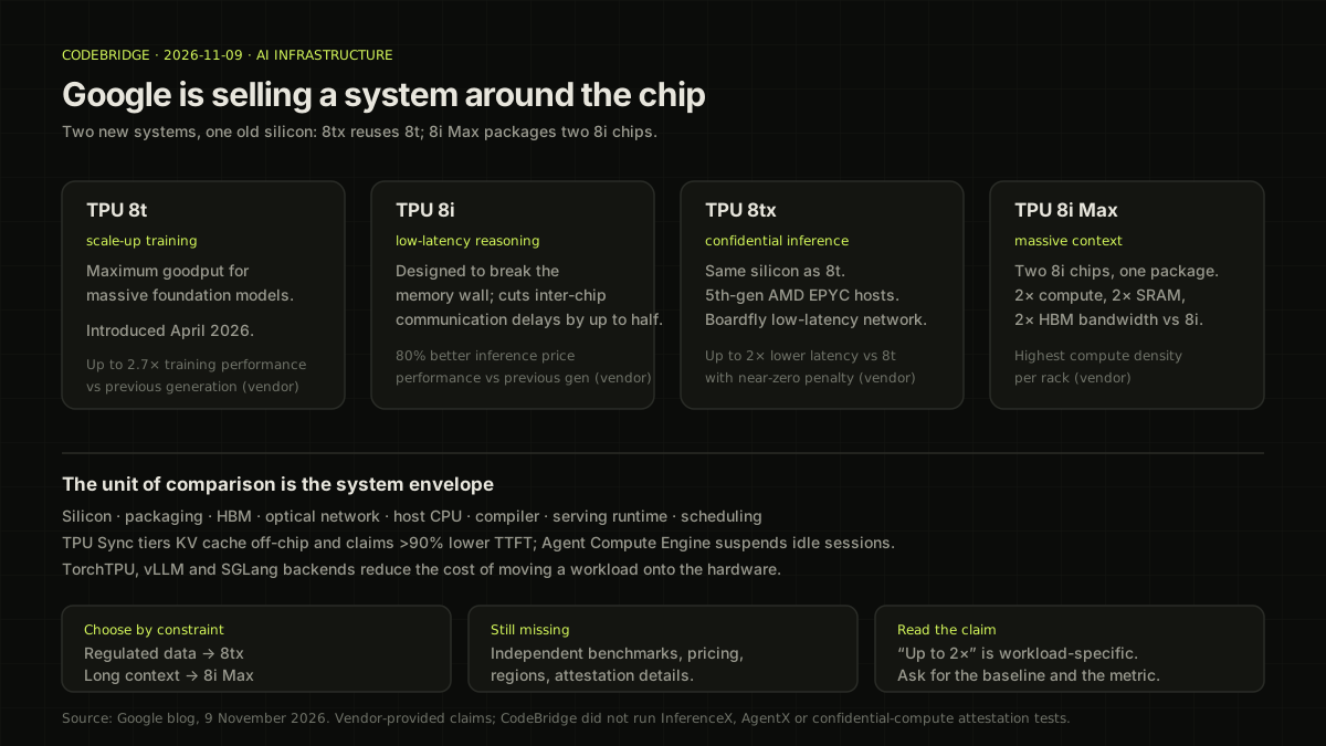
The eighth-generation TPU portfolio has four entries. 8t targets large-scale pretraining, 8i targets real-time inference, 8tx targets confidential inference, and 8i Max targets very large context and the highest compute density per rack. Google says this is the first time it has introduced four TPU systems in a year.
| System | Stage it targets | Key composition | Published claim |
|---|---|---|---|
| TPU 8t | Large-scale training | Eighth-generation training chip | Up to 2.7× training performance over the prior generation |
| TPU 8i | Low-latency inference | Eighth-generation inference chip | 80% better inference price-performance over the prior generation |
| TPU 8tx | Confidential inference and small-scale training | Same silicon as 8t, fifth-gen AMD EPYC hosts, Boardfly | Up to 2× lower latency than 8t, near-zero performance penalty |
| TPU 8i Max | Very large context and highest density | Two 8i chips in one package | 2× compute, SRAM and HBM bandwidth over 8i |
Every number in that table comes from Google. CodeBridge did not run InferenceX, AgentX or confidential-computing attestation. "Up to 2×" depends on the baseline and the workload.
8tx: same chip, different security contract
The point of TPU 8tx is not a new chip but a way to place the same chip in a confidential-computing environment. Data is normally encrypted at rest and in transit but decrypted in memory while a processor works on it. 8tx claims to protect and isolate sensitive data and model weights at the hardware layer even while they are in use.
The composition is systemic. Google pairs the same silicon as 8t with fifth-generation AMD EPYC CPU hosts and attaches Boardfly, the low-latency network built for real-time inference. The result is a claim of up to 2× lower latency than 8t with "near-zero performance penalty." Because it combines training-grade compute with a fast inference network, Google says customers can fine-tune on private data, distill a large model into a smaller one, and train agents with reinforcement learning without moving sensitive data to a separate cluster.
Three things would need to be checked before that claim means much. First, the threat model and attestation method for confidential computing. Second, how much of the data path between host CPU and accelerator is protected. Third, which workload produced "near zero." Security is not a feature list; it is an attack surface and a key-management problem.
8i Max: pushing the memory wall into packaging
8i Max solves a different problem. When several agents work through one codebase or hours of video at the same time, memory bandwidth becomes the bottleneck. Google puts two low-latency 8i chips in one package so compute and memory scale together. It claims 2× compute, 2× SRAM and 2× HBM bandwidth over 8i, so the processor keeps the data it needs close by.
Density is part of the pitch. Fitting twice the silicon into the same rack space lets a data centre place more compute per square foot and per watt. That is bound up with power, cooling and rack design, so how "2×" shows up in operating cost needs separate verification.
The real competitiveness of 8i Max is not the FLOPS of one chip. It is how efficiently the memory hierarchy is used when handling very large context. In the same announcement Google open-sourced TPU Sync. It presents HBM, host DRAM, shared storage and the data-centre network as one memory hierarchy, tiers large KV caches off-chip in milliseconds, streams context between disaggregated prefill and decode nodes, and synchronises RL weights. Google claims this cuts KV-transfer latency and time to first token by more than 90%.
Software is half the system
The easy part to miss in this announcement is the software. Google open-sourced TorchTPU so PyTorch code and Hugging Face models run natively on TPUs, with vLLM and SGLang backends. The TPU agent suite attaches to coding tools such as Claude Code, Cursor and Google Antigravity to handle TPU onboarding, bottleneck diagnosis and kernel autotuning in natural language. XLA Serving Engine serves models trained in Python through a low-latency C++ runtime.
Agent-fleet operations are also a software layer. Agent Compute Engine automatically suspends and resumes idle sessions while stateful agents wait seconds or hours for a database lookup, an external tool or human feedback, cutting infrastructure cost. Cloud Pathways lets GKE treat multiple TPU slices as one local machine, and GKE dynamic slicing reconfigures topology on the fly with optical circuit switching, which Google says cuts job start time by up to 5× and failure recovery by up to 4.5×.
None of this appears on a chip spec sheet, but it can affect real agent operating cost more directly. A model can be fast and still waste money if idle sessions hold TPUs. A great chip can still produce a bad experience if time to first token spikes when the KV cache leaves the chip. Infrastructure choice is no longer "which chip is fastest" but "which system handles my workload's bottleneck most cheaply."
What is still missing
The announcement has no pricing, regions or exact availability dates. "Nearly 100 customers" is Google's phrasing, and the customer mix and workload share are not disclosed. The power and thermal design of 8i Max, the attestation details of 8tx and the real topology of the Boardfly network all need more evidence.
"Up to 2× lower latency" and "near-zero performance penalty" may also come from different baselines. Whether the comparison is against 8t or 8i, and which model, batch size and sequence length were measured, changes the result. Vendor blog numbers are useful for direction, but an adoption decision needs a pilot on your own workload.
Insight: compare the envelope, not the chip
The lesson from TPU 8tx and 8i Max is not that Google builds better chips. It is that the same silicon, bound with different packaging, networking, security and software, becomes a different product. 8tx targets data sovereignty in regulated industries. 8i Max targets the very large context of agents. Neither is explained by a chip's performance table alone.
When evaluating infrastructure, look at silicon, packaging, HBM, the optical network, host CPU, compiler, serving runtime and scheduling as one envelope. Define where your workload's bottleneck sits inside that envelope—security, context length, idle sessions, KV-cache movement—before concluding that "the TPU is fast."
For the cost structure of model routing, continue with Muse Ember. For the memory boundary of a local model, see Nota AI's 1.58-bit 30B.